

👋 Happy Saturday! This week’s highlights include lecture notes on the semiconductor ecosystem and its shift to advanced packaging, a map of Silicon Valley’s early talent clusters, and a video showing the absurd complexity of cracking an egg by machine.
Interesting Lecture Notes: The Semiconductor Ecosystem Pyramid
The semiconductor supply chain looks like a pyramid with raw materials and chemicals at the base, equipment suppliers in the middle, foundries and IDMs fabricating chips above that, and end products at the top. From IEEE’s lecture notes on advanced packaging, packaging isn’t just a protective shell anymore - it’s a key performance multiplier.
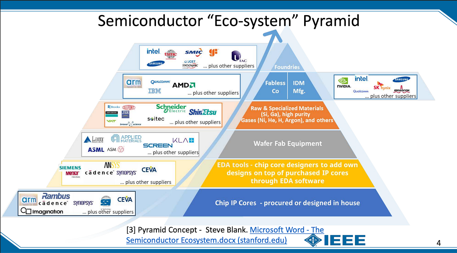
Advanced packaging has been around in some form since the 1990s (flip-chip, wafer-level packaging, through-silicon vias), but it only became strategically central in the last 10–15 years as Moore’s Law scaling slowed. Instead of squeezing more transistors onto a single die, companies began using techniques like 2.5D interposers, high-bandwidth memory stacks, and eventually chiplets to stitch multiple smaller dies into one package. AI accelerators and EV power electronics both depend on it today, and packaging capacity is growing faster than front-end fabs.
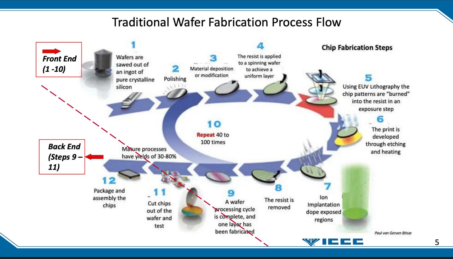
The interesting shift here is that tools usually associated with transistor scaling (thin-film deposition, lithography, polishing) are now being retooled to stitch dies together. The same capital equipment that once enabled Moore’s Law scaling now underwrites the chiplet era. A relevant example: Apple’s M1 Ultra isn’t a monolithic die, but two M1 Max chips linked through a silicon interposer Apple brands as ‘UltraFusion’.
Watch the video in the original issue.
Interesting Photo: A Cartography of Silicon Valley
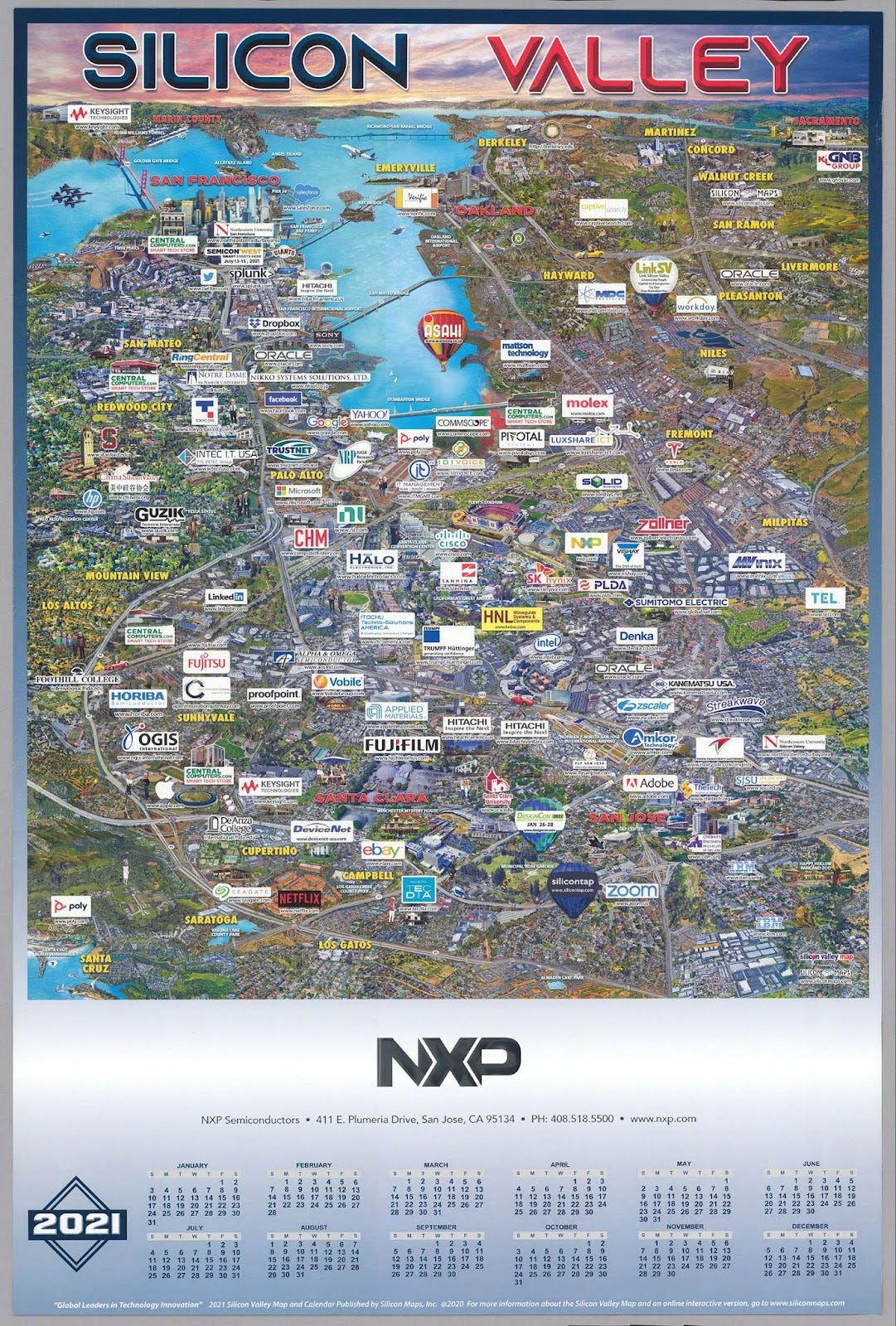
This old-school map shows the dense web of semiconductor and computer companies that built Silicon Valley from its earliest days. Talent clusters work like this: competitors set up next to each other because co-location makes it easier to hire specialized engineers, share knowledge, and stay close to the state of the art. The same pattern played out in Detroit with legacy automotive manufacturing, to some extent in Shenzhen with consumer electronics and contract manufacturing, and more recently in El Segundo, where aerospace and space startups have spread across the broader LA area.
You can trace the full lineage of Silicon Valley companies back to the early 20th century in this map archive; also see Issue #131 for a map of emerging hard-tech companies across Southern California.
Interesting Video: Building an Automatic Egg Cracker
A wildly overbuilt solution to cracking an egg? Another classic project from Stuff Made Here.
Tangentially related but much simpler: the German Eierschalensollbruchstellenverursacher does the same job for soft or hard-boiled eggs with a spring-loaded weight. Here’s a video demo of the device in action. The name is a literal translation of ‘eggshell predetermined breaking point causer.’
Manufacturing & Startup News
More leftovers from our weekly research:
- Hades Mining raised $6M in pre-seed funding to develop proprietary drilling technology for ultra-deep geothermal energy and critical mineral extraction using in-situ recovery processes.
- Astrus secured $8M in seed funding to advance its AI platform for automating analog chip layout with physics-aware simulations.
- Yottar raised $1M in pre-seed funding for software that analyzes grid-connection data to identify viable sites for renewable energy projects under capacity constraints.
- Hyperdrives raised $3.3M in seed funding to develop high-performance electric motors for automotive and industrial applications, improving the efficiency and power density from incumbent solutions.
- Oxford University spinout OrganOx was acquired by Terumo Corporation for $1.5B. OrganOx develops organ preservation technology for kidney and liver transplants using normothermic machine perfusion.