

Topics worth your time this issue: Claude learning the CAD process, a backyard Class 100 fab making RAM, the rise and fall of Boosted Boards, a practical guide to snap-fit design, and space station telemetry.
Interesting Diagram: Claude & The CAD Process
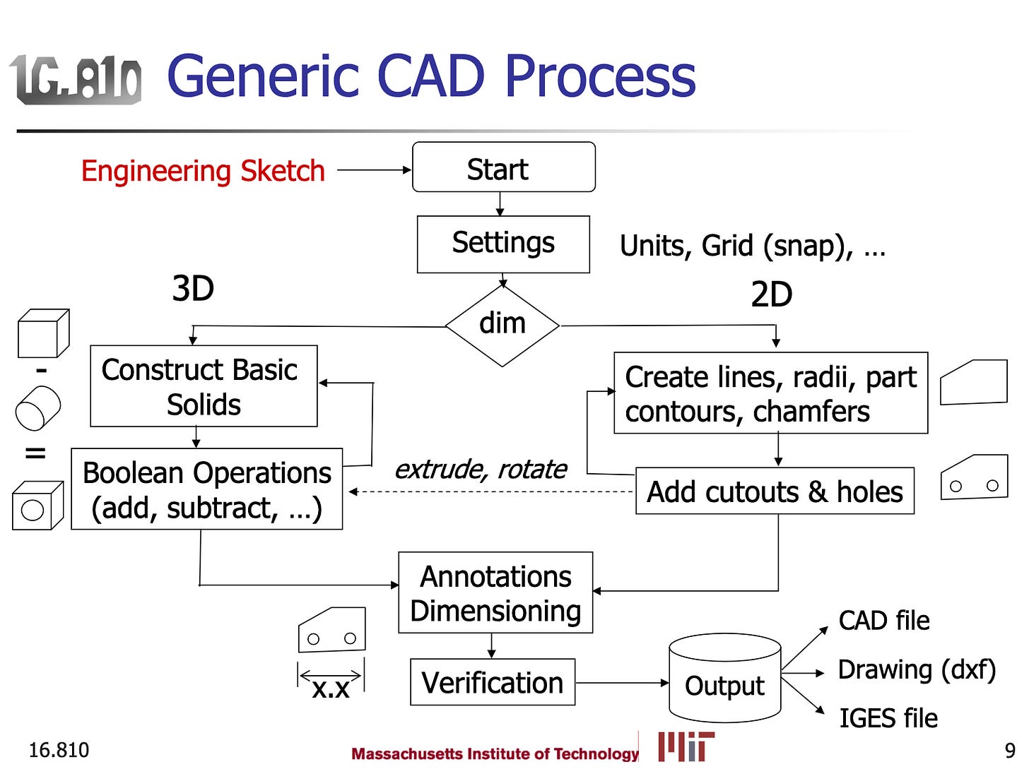
A simple flow diagram mapping how a hand sketch becomes a CAD model. The source material gets into the older bones of computer-aided design: IGES as an early neutral file format, vector geometry for editable shapes, and the curve math behind smooth surfaces (Béziers, B-splines, NURBS).
A useful companion piece is this Onshape MCP experiment on how capable Opus 4.7 is as an AI model. The author had it build a four-part monitor arm from a sketch and short written description, producing a structured feature tree and iterating through Onshape with enough visual feedback to inspect its own work. The key was to describe the design intent clearly and with enough tools to check what it had built:
Not “autonomous CAD” (we’re not there yet), but “CAD copilot driven by design intent.” You describe what you want in plain English. Claude produces a feature tree. You sanity-check it, maybe correct a mis-read, and then it builds. The workflow replaces keyboard shortcuts and feature-tree surgery with typing and verbal iteration. If you already know what you’re building, Claude is remarkably fast at building it. As usual with early AI tools, the first step to building something is being able to describe what you want to build.
Here’s the same plugin used to compete in SolidWorks Model Mania 2025:
Watch the video in the original issue.
The shared lesson in both: CAD is not about “drawing on a computer”; it’s a stack of geometric representations built to make design intent editable, transferable, and eventually manufacturable.
Interesting Video: Building a Class 100 Fab in a Backyard Shed
Another entry in the lineage of home-built production facilities, this is perhaps the most ambitious build we’ve come across: a Class 100 semiconductor clean room, built inside a backyard shed, now being used to fabricate RAM.
His facility doubles as a visual walkthrough of the semiconductor manufacturing process at each stage and the core steps — plasma etching, high-temperature processing in a vacuum furnace, i-line lithography built from a modified microscope, automated sample cleaning, fume hood work, and thin film deposition.
The ongoing RAM shortage has put memory supply chains back under scrutiny, and while this isn’t a production-scale facility, it is a working, end-to-end process line for the same device class built entirely from personal capacity.
(Class 100 refers to fewer than 100 particles ≥0.5µm per cubic foot of air; this is one of several cleanliness standards used in commercial fabs.)
More From Around the Web
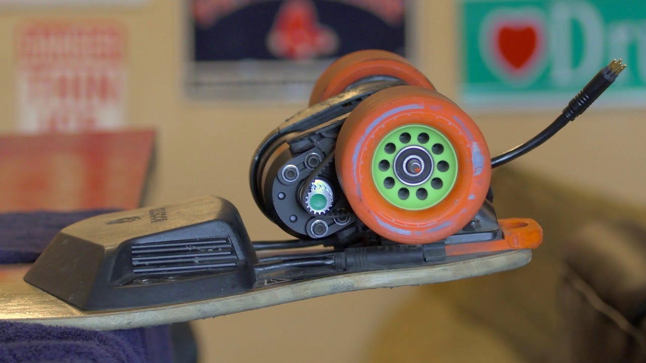
- For weekend listening, a classic episode on the rise and fall of Boosted Boards. Good lessons on how hardware startups can get trapped between scale, capital, and operations.
- ISS bathroom tank telemetry, taken to its logical extreme.
- Emosh from WORC shared a public breakdown of mathematical snap-fit design. Bayer Material Science’s Snap-Fit Joints for Plastics is the golden reference.
- A contrarian take from George Hotz: AI has no moat.
- A short history of the Torx screw.
Manufacturing & Startup News
More leftovers from our weekly research:
- Twelve, a startup producing synthetic aviation fuel from captured CO₂, started commissioning its Moses Lake SAF plant and is reportedly planning a Series D after first shipments.
- Schematik raised $4.6M in pre-seed funding to build a “Cursor for hardware” that turns project descriptions into code, wiring diagrams, component lists, and assembly instructions.
- Crewline raised $7.1M in seed funding to deploy an autonomous retrofit kit for construction rollers, using soil compaction as its entry point into earthwork automation.
- Bubble Robotics raised $5M in pre-seed funding to build long-duration autonomous robots for subsea inspection and monitoring.
- A&K Robotics raised $8M CAD in Series A funding to develop a self-driving indoor mobility robot for moving passengers through airport terminals.