
There’s been a lot of talk lately about reindustrializing America. Between the CHIPS Act, reshoring incentives, venture-backed manufacturing startups, and even the latest YC manifesto, the message is clear: America should build more of its own stuff, including electronics. But what does that actually look like?
We recently had the chance to see for ourselves, touring one of Summit Interconnect’s quick-turn PCB shops where commercial prototypes are built in just 1 to 3 days. These are the boards used in prototyping and low-to-medium volume production: small batches, tight timelines, and no room for delay. There’s a good chance your prototype boards were built in a shop like this, in the kind of place that cranks out quick-turn PCBs for everyone from weekend tinkerers to massive organizations spending millions a month in R&D.
It’s worth noting that this is one of Summit’s prototype-focused sites, not the high-volume production lines they run elsewhere. What follows is a photo-heavy walkthrough of how a bare PCB gets made from raw laminate to final inspection. If you've ever wondered what happens between “upload Gerbers” and “board arrives in the mail,” this is the process.

Printed circuit boards are fabricated here in Hollister, California, across two facilities totaling nearly 30,000 square feet tucked past patchworks of fields and low-slung hills on the edge of town.
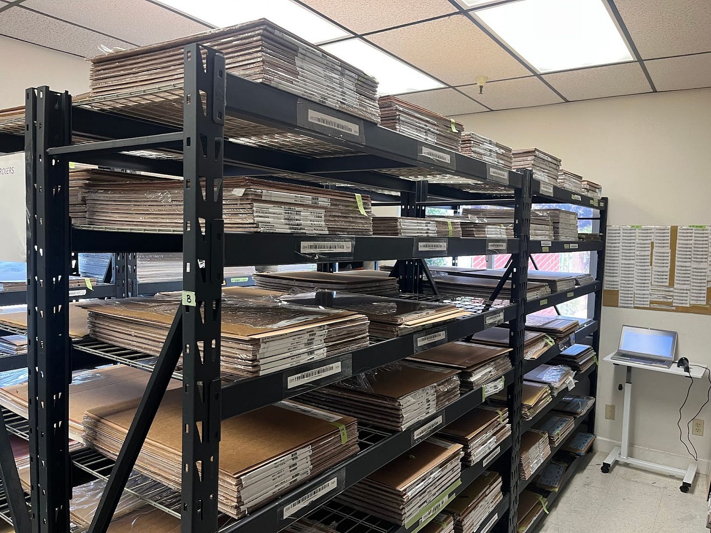
The fabrication process starts with defining the board stack-up: a layer-by-layer specification that determines the board’s materials, thicknesses, and sequence. It’s essentially a recipe for the PCB, and pulled directly from the material traveler that follows each order through the shop.
Think of a PCB as a multi-layer sandwich of copper and insulating material. The copper forms signal traces and planes, while the insulating layers—usually made from fiberglass-reinforced epoxy or commonly referred to as FR4—set the spacing and give the board its structure. These layers come in two forms: core, which is a rigid sheet of fully cured FR4 with copper foil on both sides (like a thin two-layer PCB), and prepreg, which is the same material in a partially cured state that melts and bonds the layers during lamination. Depending on the design, a board might have 4, 8, or 20+ layers.
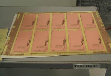
Walk a few rooms past the raw material racks and you’ll find yourself in a yellow-lit room. It looks a bit out of place, but there’s a very good reason for it: this is the photolithography area. This step defines where copper will stay and where it will be chemically removed. It’s done using dry-film photoresist and laser direct imaging (LDI), a photolithography process scaled for 18" × 24" copper panels instead of wafers.
Dry-film photoresist is UV-sensitive, so the entire room is lit with filtered yellow light to avoid unintentionally exposing the panels. It’s the same reason photoresist rooms in semiconductor fabs have amber lighting.
Inside, you’ll see:
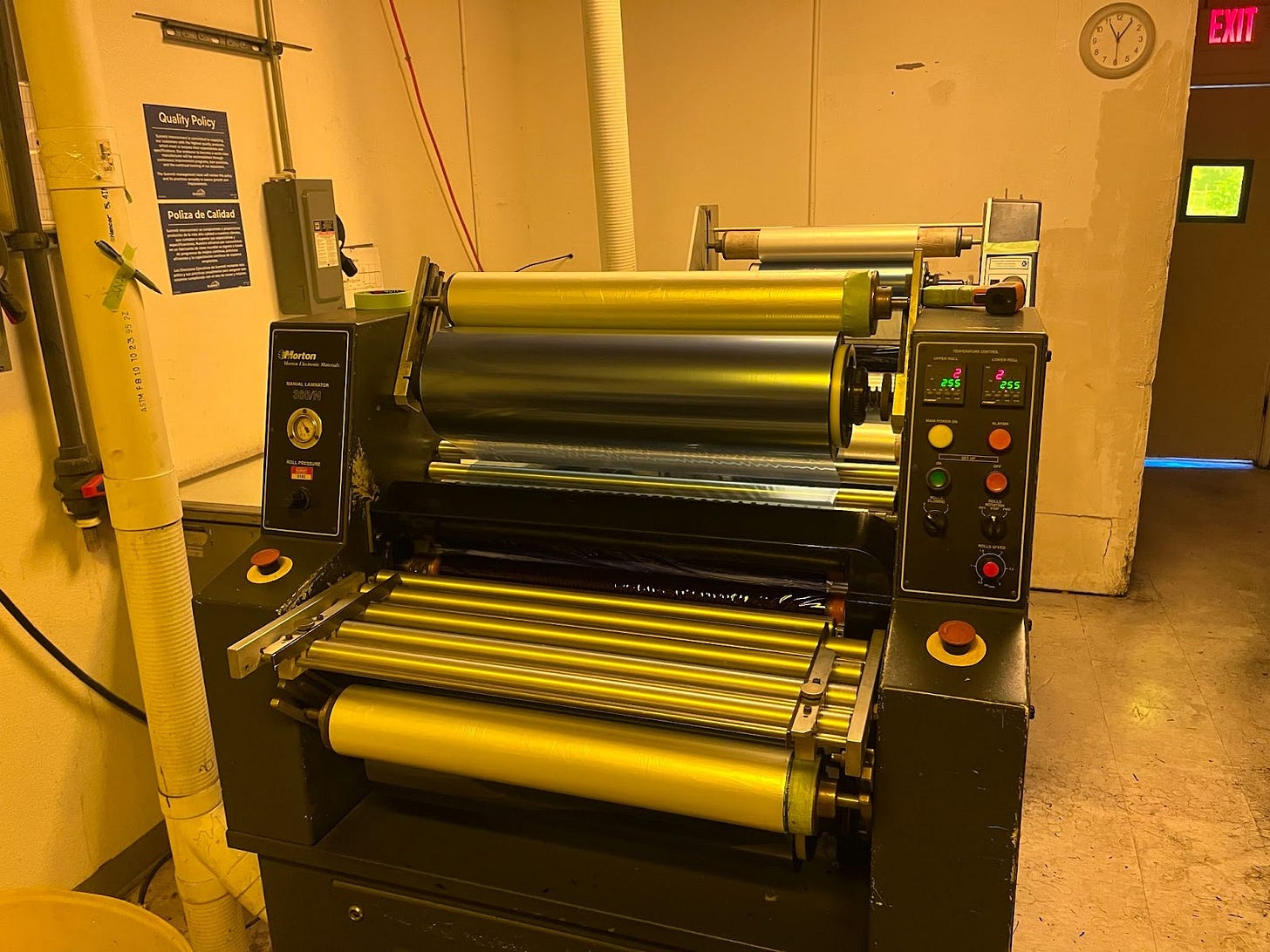
A roll laminator, where dry-film resist is applied to each inner layer copper-clad panel under heat and pressure. This step preps the inner layers for imaging.
A laser direct imaging system where a UV laser scans across the panel to expose the trace pattern. Nothing visibly changes at this stage, the resist simply hardens in the exposed regions.
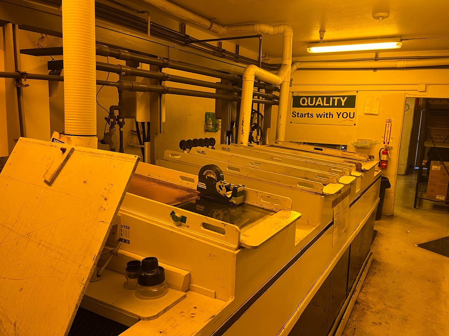
And after imaging, a wet process line for image development. Here, a mild alkaline solution removes the unexposed photoresist. These are the areas that weren’t imaged by the laser and remain uncured. The exposed areas, hardened by the laser, stay intact and protect the copper traces. Everything else, effectively the unprotected copper, gets etched away in the next step.
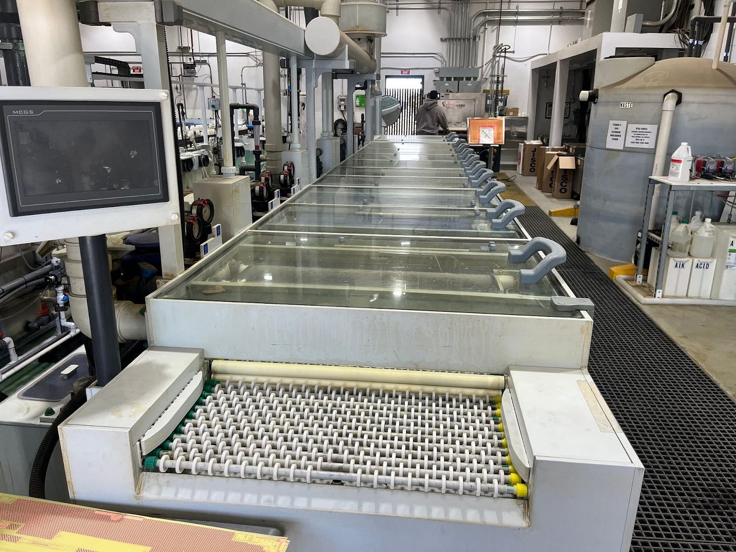
Outside the room, you’ll find a massive section of the facility dedicated to wet chemical processes with long rows of conveyorized tanks. Here, the panels enter the etching line where a cupric chloride solution removes the unprotected copper.
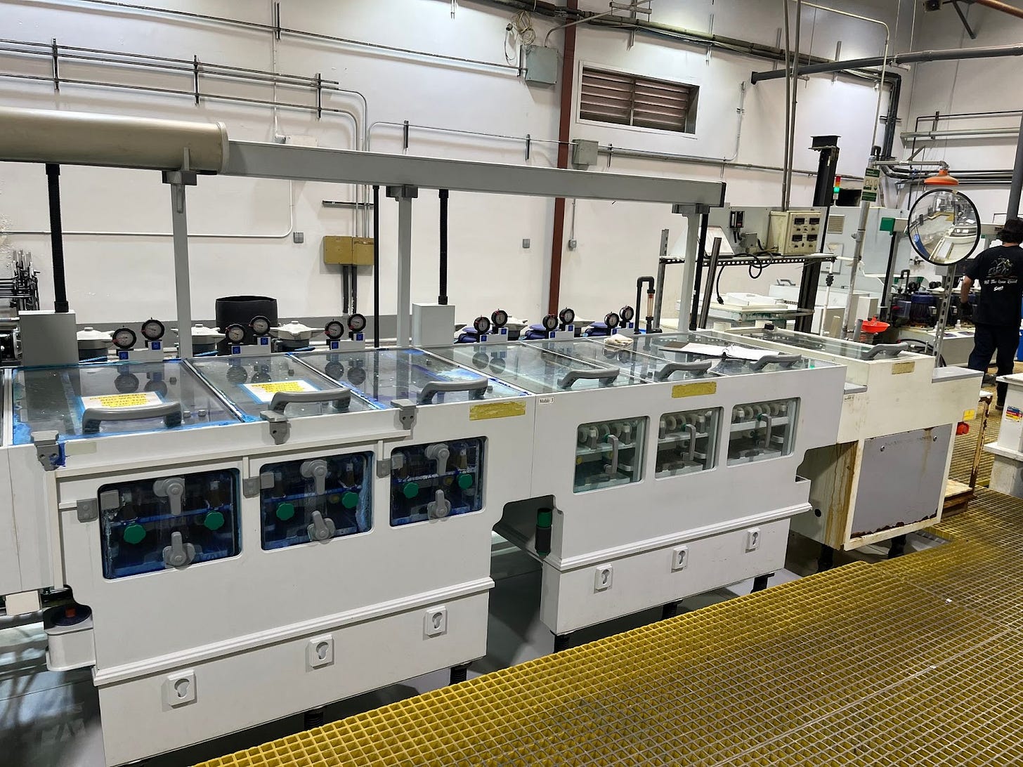
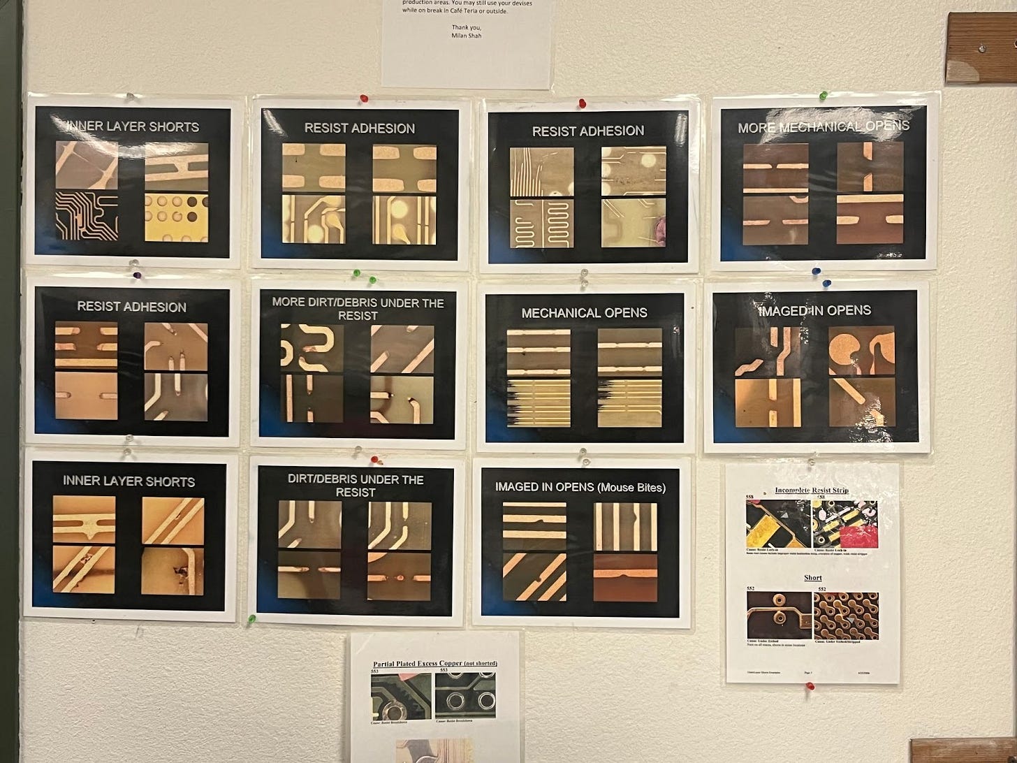
After imaging, each layer goes through automated optical inspection where machines look closely for defects like opens, shorts, nicks, pinholes, or leftover debris. AOI systems use high-resolution cameras and structured lighting to scan the copper surface, then compare those images against the original Gerber data. Think of it as a 2D image-based verification process, tuned for fine-line resolution down to 2–3 mils depending on the system.
Any suspect regions (missing traces, extra copper slivers, incorrectly etched features) are logged and presented to an operator for manual review before the board moves on. This is a critical checkpoint before lamination since defects here get locked inside the board and can’t be fixed later.
Before inner layers can be laminated together, the copper surfaces go through a brown oxide treatment step. This process prepares the copper to bond with the prepreg resin during lamination.
Panels are run through a chemical bath that microscopically roughens the copper and deposits a thin layer of cupric oxide (or an equivalent compound). The modified surface has increased roughness and better chemical compatibility, which improves adhesion to the epoxy.
The result is a matte, reddish-brown finish on the copper strictly for adhesion purposes. Skipping this step risks delamination, especially under thermal cycling or mechanical stress.
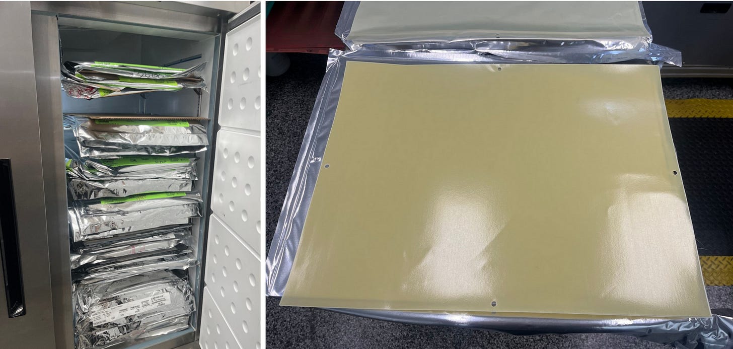
Layup and lamination take place in a temperature and humidity-controlled area. Prepreg, the fiberglass sheet pre-impregnated with epoxy resin, is sensitive to both heat and moisture. Temperature control prevents the prepreg resin from curing too early, while humidity control keeps the material from absorbing moisture.
To layup a board, operators build the stack layer by layer with alternating inner layers and prepreg, then cap the stack with copper foil for the outer-layer. In prototype and quickturn facilities like this, layers are either manually aligned using alignment pins or are aligned using a pinless lamination system.
The stacks then go into a lamination press, where heat and pressure cure the resin and bond the layers together. If multiple boards share the same stack-up (e.g. prepreg material), they’re pressed in the same cycle.
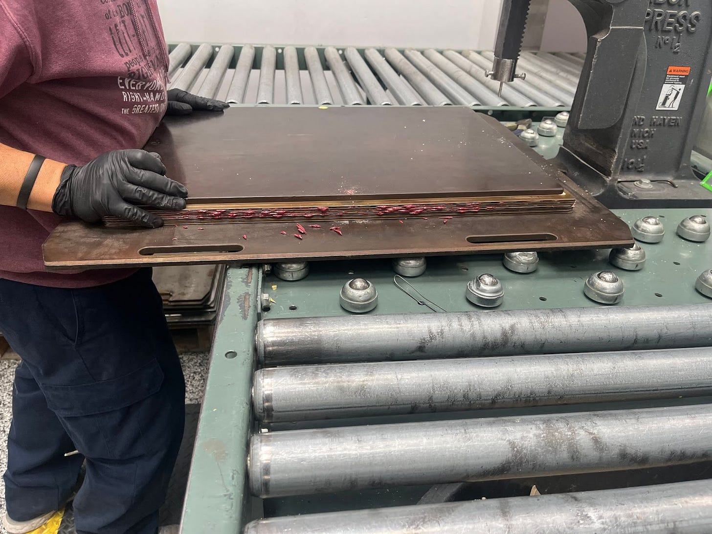
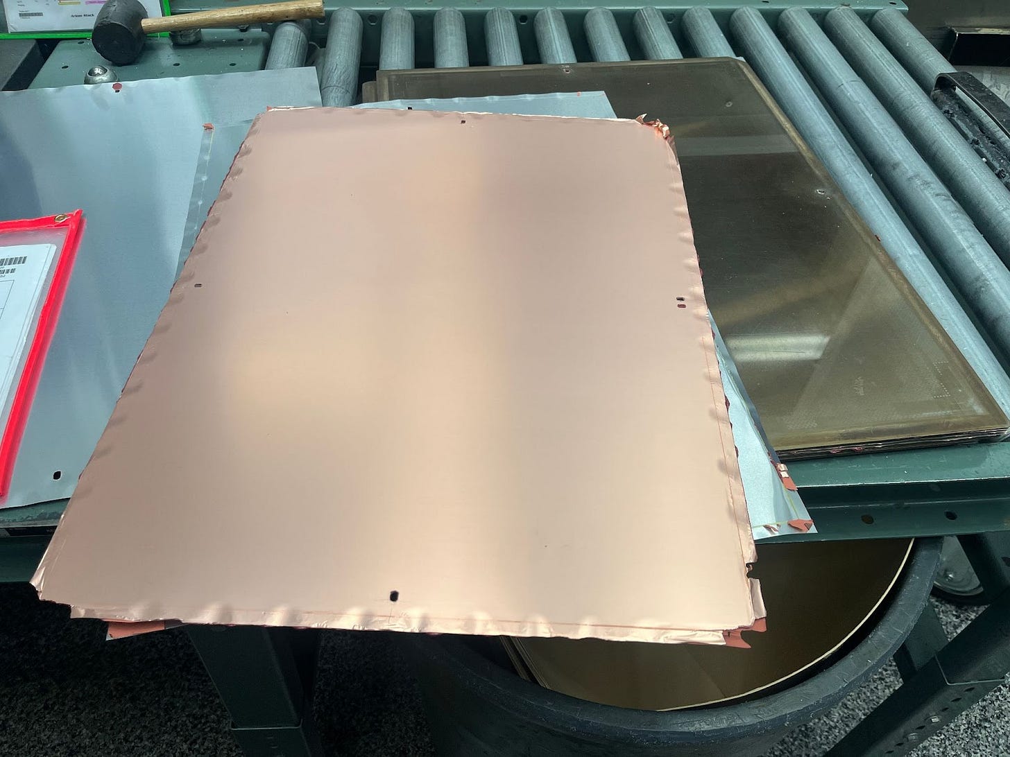
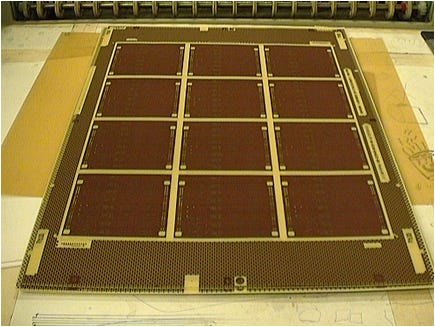
After layup and lamination, the panel edges are trimmed to a standard size. The result is still just a bare laminate with an unpatterned outer copper layer and no drilled or plated vias.
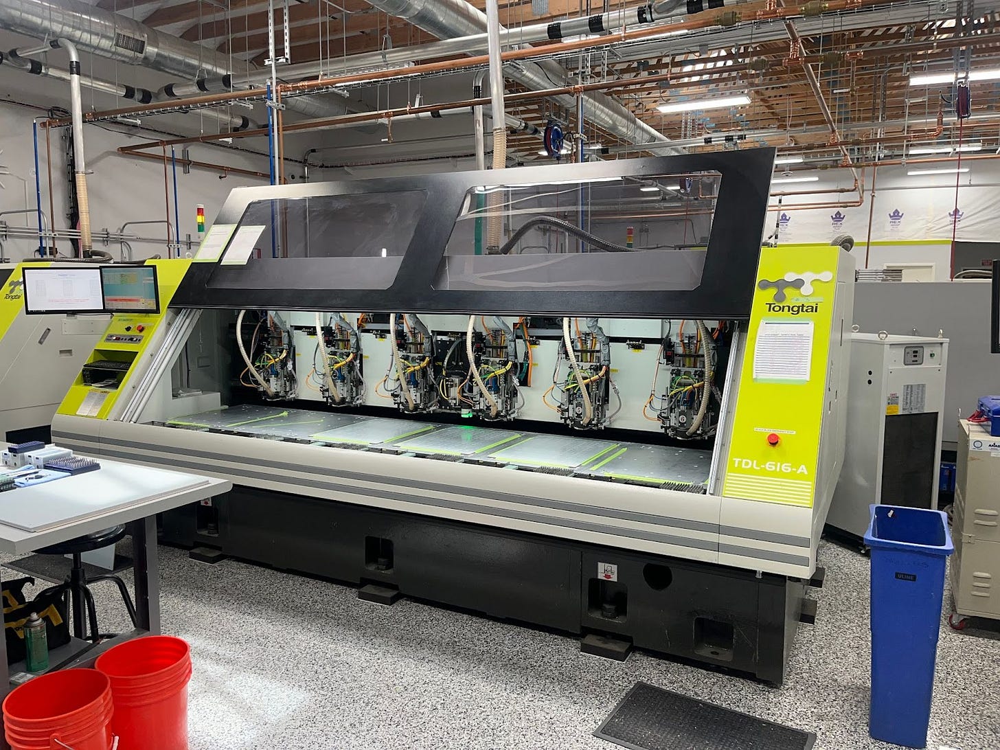
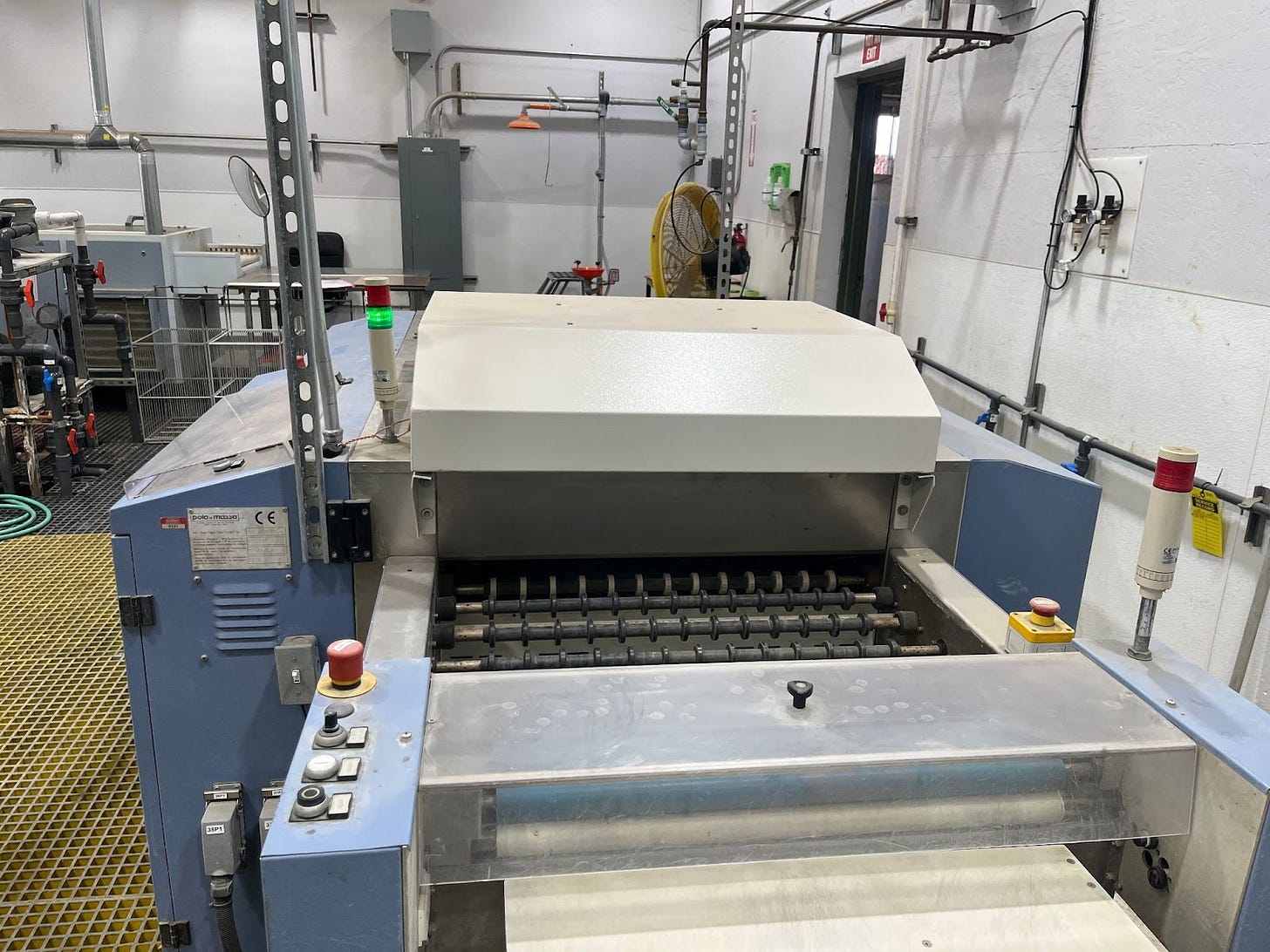
The next step is to create vertical interconnects (commonly referred to as vias) that electrically link copper features between layers. These are precision-drilled holes that will later be plated with copper to form conductive paths. Without them, the layers are just isolated sheets of copper and dielectric.
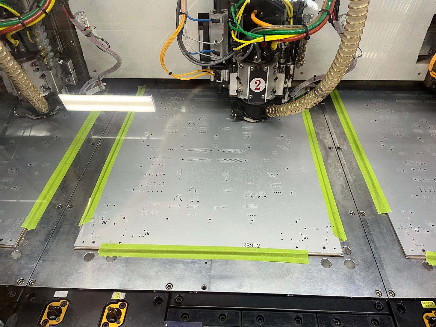
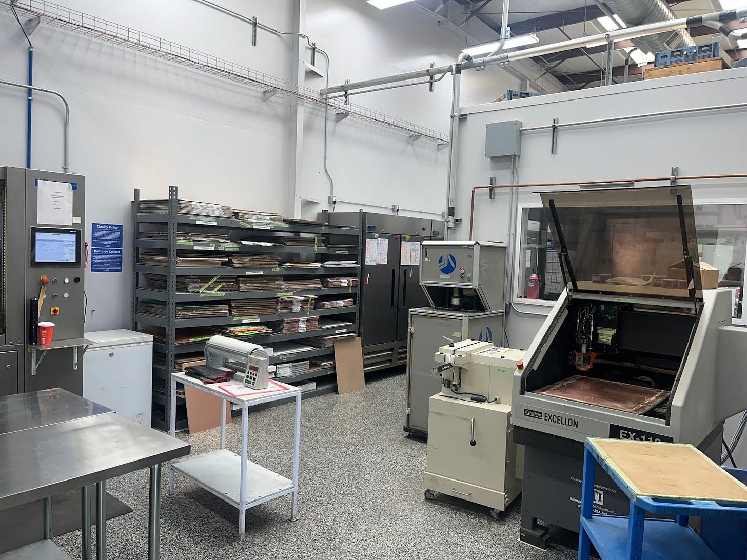
A via is just a tiny copper-lined hole that lets signals (or power/ground) travel vertically from one copper layer to another. Some go all the way through the board (through-hole vias), others stop halfway (blind/buried vias), but they all start the same way: either a CNC drill bit cutting precise holes in the stack or, for microvias, a laser ablating them.
Drill size and accuracy matter. Plated holes that carry signals, power, or ground between layers have a tolerance of ±3 mils. Non-plated holes, like mounting points or tooling holes, are even tighter at ±1 mil.
You’ll usually see racks of spinning drill heads or a bit carousel swapping out tools mid-job. Each bit is dialed in for a specific hole diameter, and there might be dozens of sizes per panel.
For even smaller features like in high-density interconnect boards used in smartphones and aerospace, Summit’s Hollister facility uses lasers to create microvias. These are ultra-fine holes, typically just 3–6 mils in diameter and far smaller than what a mechanical drill can achieve. They’re used to connect adjacent layers in dense, space-constrained designs.
After drilling, the panels need to be cleaned and conditioned before any copper can be plated into the holes. The first step is deburring, which removes any leftover fiberglass or resin slivers around the edges of each hole.
Then the board goes through desmear, a chemical or plasma process that removes the thin film of melted epoxy left behind on the hole walls when the vias are drilled. This smear can block electrical contact to the inner-layer copper, so it has to be stripped off to ensure a reliable connection when the vias are plated.
After cleaning, the holes are still non-conductive. That’s where direct metallization comes in. A thin seed layer of conductive material, often a carbon-based or palladium catalyst, is deposited on the hole walls. This creates a continuous path for current so that the electroplating process can later deposit copper inside the vias.
With the holes drilled and a thin seed layer deposited, the board is ready to build up its final copper.
First, a dry-film photoresist is applied to both outer layers and imaged using the same LDI system from earlier. This defines where traces and pads will go, but unlike the inner layers, the board isn’t etched right away. Instead, the exposed copper is electroplated, adding more copper to the trace areas and inside the vias. Immediately after, a thin layer of tin is plated on top. This tin serves as an etch mask.
Copper electroplating step: an electric current deposits copper onto all conductive surfaces, thickening the outer layers and fully lining the via walls.
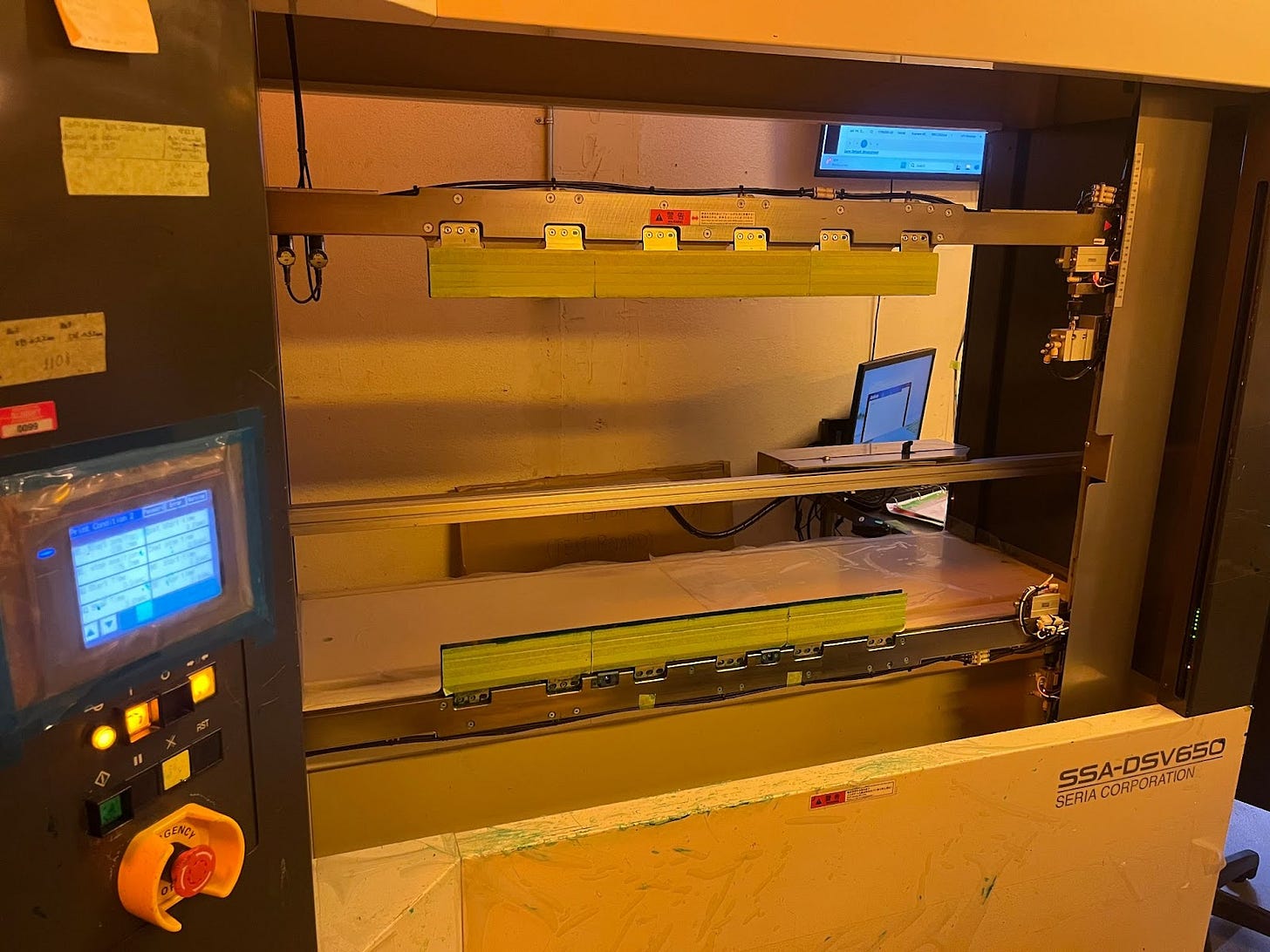
Standard green soldermask is run on a Seria SSA-DSV650, a vertical double-sided screen printer used for automation. Panels are clamped upright and coated on both sides in a single pass. The machine controls squeegee pressure and speed down to fine increments, which helps maintain a consistent film thickness.
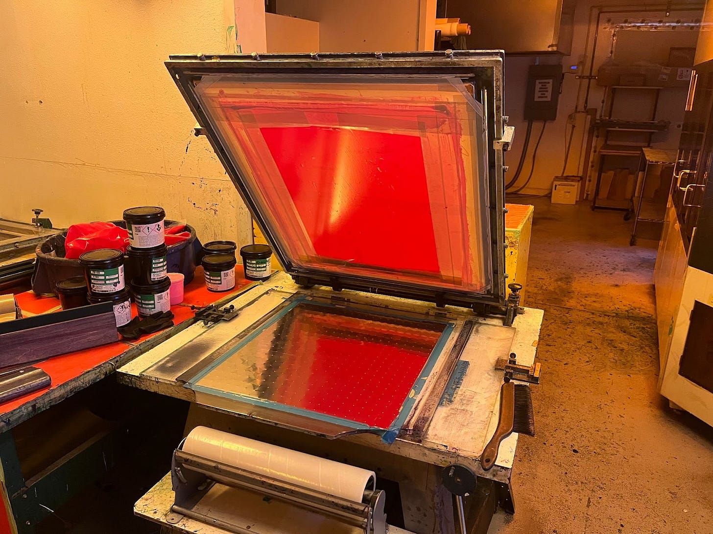
Custom colors get routed to a manual screen printing table. A technician floods the mesh and pulls a hand squeegee across each side. Slower, but flexible, and you don’t have to flush the entire automated line just to change colors.
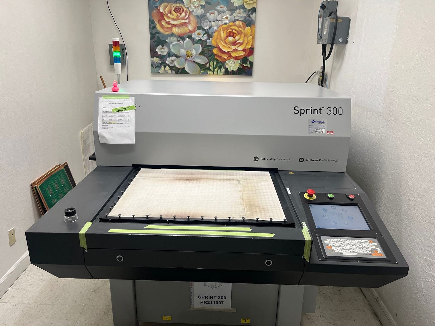
Legend comes last. It’s traditionally called silkscreen, and it’s applied using a Sprint 300, essentially an inkjet printer for circuit boards. This layer adds part numbers, logos, and labels for test points. As it prints the white ink is tack-cured instantly, so the panel comes out dry and ready for a final bake.
Once the legend is printed and cured, each panel goes through electrical test. This shop uses a flying probe tester, a machine that moves high-speed test needles across the panel to check for opens, shorts, and misroutes. The probes follow the board's netlist and position data directly, which makes it slower than a bed-of-nails setup but much more flexible for high-mix or quick-turn jobs.
Finally, after testing the boards go to routing, where each individual board is cut out of the larger panel, followed by a final inspection before packaging and shipping.
PCB fabrication is a finely tuned process with dozens of carefully orchestrated sequences. We didn't touch on every step, like applying surface finish (ENIG) where exposed copper pads are plated with nickel and gold, or the numerous quality checks embedded throughout the process. But from raw laminate to finished bare board, this is the full process.
Huge thanks to Allison Herrera (our guide and Summit sales rep), Jon Lass (GM of the Hollister facility), and Lisa Holmes (marketing) for making this tour happen and letting us share their story. After walking the floor and meeting the team, including the original shop owner and technicians with over 20 years of experience, it's clear this place embodies the depth of experience that defines so many great North American manufacturing floors.

