Sourcing guides at HQB, gigacasting & thixomolding, chip manufacturing, frangible nuts, and more.
|No. 253|
Interesting Links
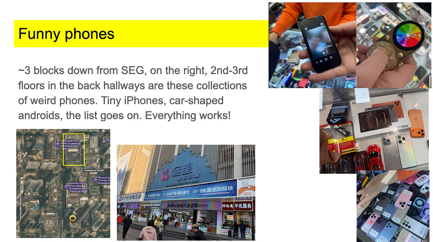
We’ve long been enamored with Huaqiangbei — the world’s largest electronics market, where you can source any component imaginable — and Andy Kong’s Huaqiangbei Guide is the best resource we’ve seen for anyone finally making the trip. Starting in 1988 as the SEG Electronics Market, HQB now spans 70M+ sq. meters across Shenzhen and is the physical manifestation of China’s electronics supply chain advantage: the density that lets a hardware team go from BOM to prototype in a day, and that famously made a from-scratch iPhone 6s possible by sourcing every component locally. One practical detail to note: most stalls showcase what factories can make, not what they stock; the real value is finding vendors who can make your specific part in a custom configuration.
If you want to see it up close, Ariel (a reader) is organizing a Canton Fair + Shenzhen trip, April 17–22. Tell her we sent you for a special discount!
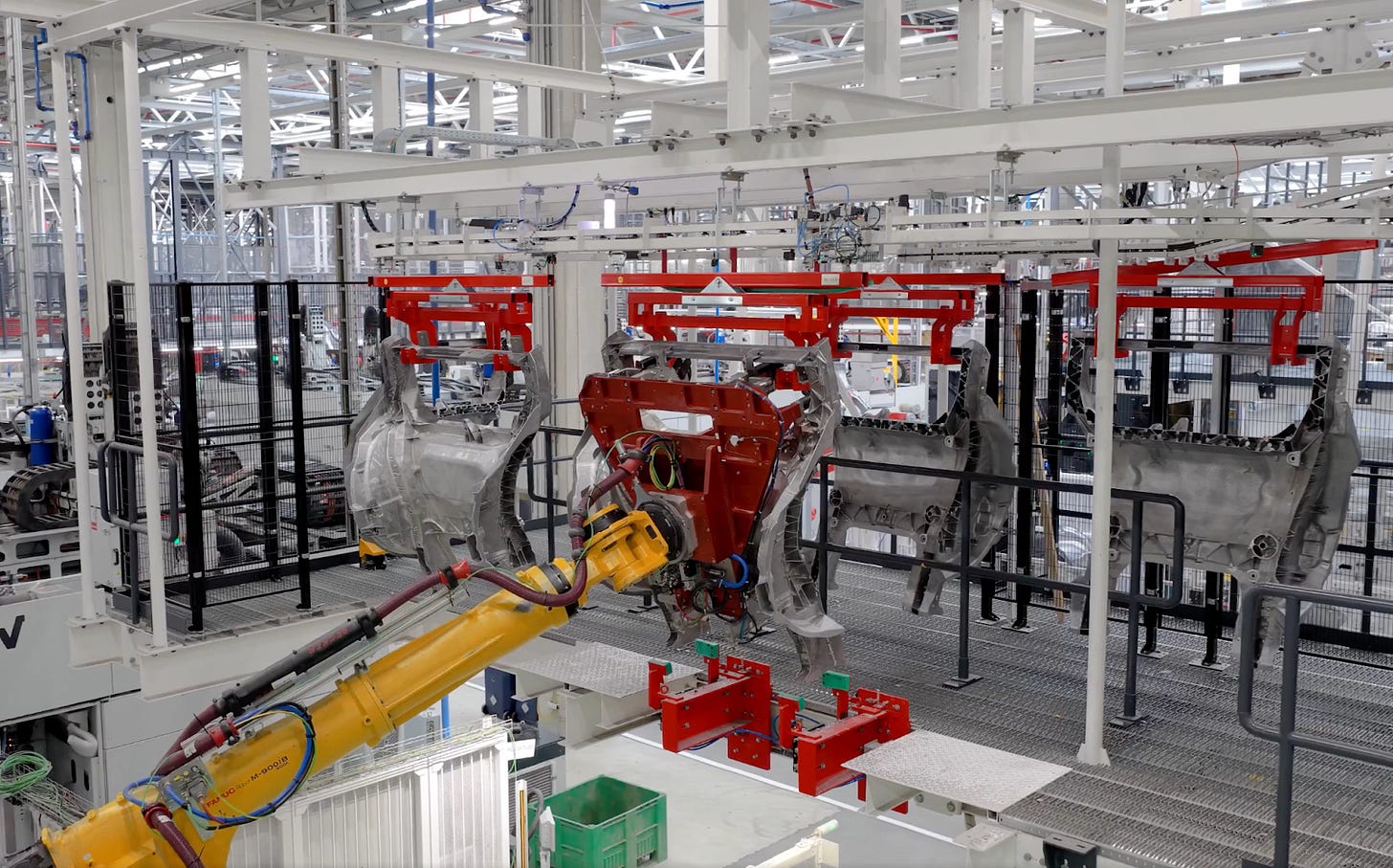
There’s a rabbit hole for every topic, including one entirely devoted to gigacasting and magnesium thixomolding called Industry Arsenal. It’s a newsletter that doubles as a living archive of OEM programs, supplier ecosystems, and the growing footprint of giga press installations. Some context on the current industry landscape: Tesla remains the furthest along with production-scale front and rear castings, while Toyota, Volvo, and several Chinese OEMs are building similar architectures into next-gen EV platforms, and others like Ford are still in the experimental phase with partial integrations. In practice, this is still largely limited to new EV platforms (not legacy fleets) where clean-sheet platforms make it easier to design around. OEMs are standardizing on EV skateboard layouts with front and rear castings, not full single-piece bodies.
Think of magnesium thixomolding as basically injection molding for magnesium (semi-solid, low-porosity), used for smaller precision parts vs. gigacasting’s large structural aluminum pieces. Tesla has a good walkthrough of the gigacasting process at its Berlin factory.
Gigafactory Berlin
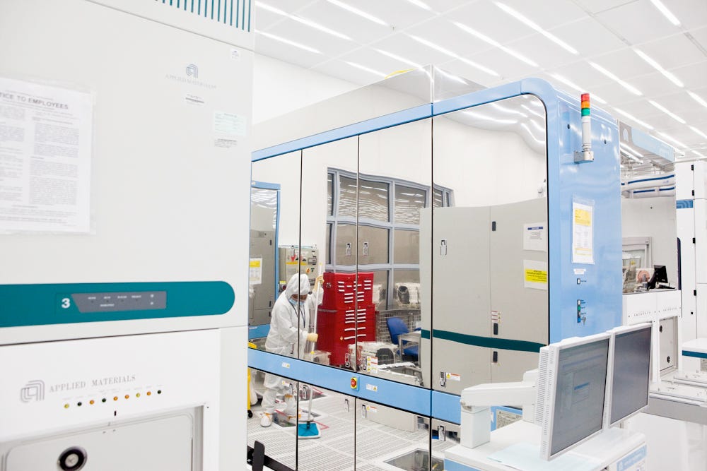
If you've ever wanted to understand what happens between a raw silicon wafer and a finished chip, The Semiconductor Chip Manufacturing Process is a solid walkthrough of the full stack. Starting with the supply chain, wafers are thin discs of highly purified silicon crystal (Shin-Etsu and Sumco make most of them) that go into fabs like TSMC or Samsung, where equipment vendors like ASML (lithography) and Applied Materials (deposition and etch) supply the machines that process them. The core loop is simpler than it sounds: deposit a material, pattern it with light, etch away what you don’t want, and repeat — 300+ process steps, across a dozen or more metal layers. The whole thing happens in high-vacuum environments and ultra-clean rooms where a single dust particle can kill a $500 chip.
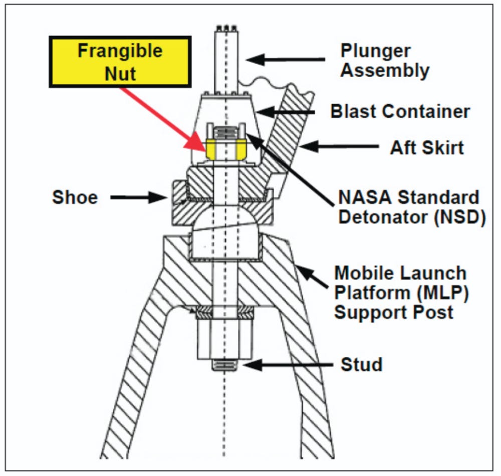
How do you build a fastener that carries structural load up to the moment you need it gone? A frangible nut is a load-bearing fastener designed to fail on command that clamps like a conventional nut under high preload, then splits cleanly into two halves when a small pyrotechnic charge fractures it. (Watch it release at shuttle ignition to separate from the launch pad). This NASA fact sheet walks through a subtle failure mode: 25 stud hang-ups across 23 launches traced to the two redundant charges firing ~250 microseconds apart. A crossover assembly tightened that to ~50 microseconds and resolved it. Both charges delivered the same total energy, but in a system as tightly coupled as a launch vehicle, microsecond-level timing differences matter.
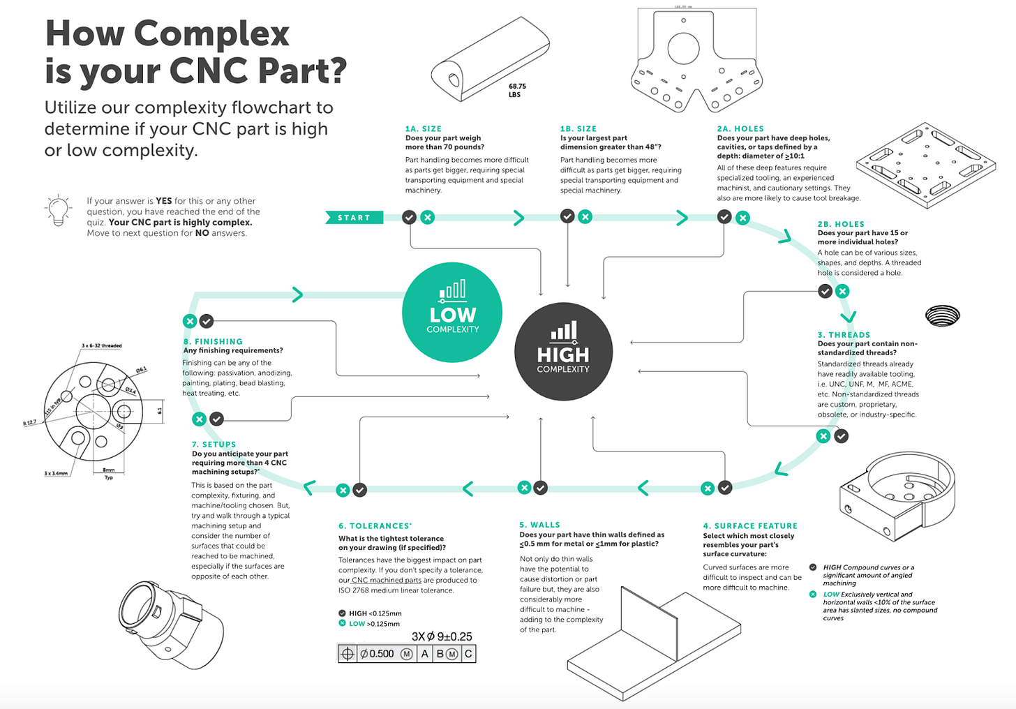
From our recent webinar with Fictiv, 60 minutes of content distilled into a single flow diagram. (High-res version available.)
Issue #120 has more examples of builds coming out of Shenzhen.
Startup News
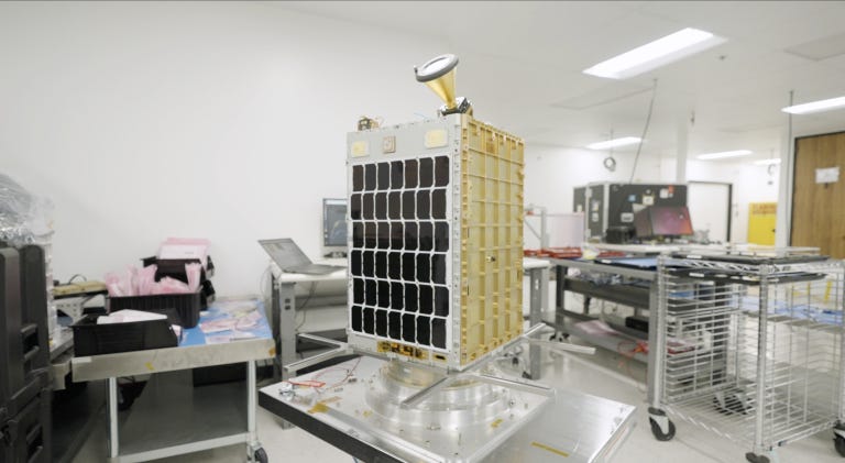
Starcloud raised $170M in Series A funding to build orbital data centers, bringing total funding to $200M and valuing the company at $1.1B. The startup has already launched a satellite carrying an NVIDIA H100 GPU and plans follow-on spacecraft with two business lines mapped out: selling compute to other satellites today and running distributed space-based data centers long-term. Their flagship vehicle is a 200 kW, three-ton spacecraft sized for Starship deployment, but an obvious caveat: Starship isn’t flying yet, and without high-cadence heavy-lift launches, space-based compute won’t be cost-competitive. In the meantime, they plan to launch smaller versions on Falcon 9. The round was led by Benchmark and EQT Ventures.
Physical Intelligence is in talks to raise roughly $1B in new funding at a valuation north of $11B for its work developing general-purpose AI foundation models for robots. The two-year-old startup, founded by former Google DeepMind researchers, has deployed its software on robotic arms to perform tasks like folding clothes, making coffee, and assembling boxes. The company had already previously raised more than $1B from investors, with Founders Fund and Lightspeed reportedly set to participate in the new round.
Benjie Holson (a roboticist at Robust AI) has a great series called the Humanoid Olympics, of which PI previously won last Fall.
Sift raised a $42M Series B round in 2025, announced last week, to expand its telemetry data infrastructure software for hardware-heavy industries. The company builds systems to ingest and structure high-volume sensor data from complex machines, with a focus on managing and exposing clean, machine-readable datasets for analysis at scale. The round was led by StepStone with participation from GV, Riot Ventures, Fika Ventures, and CIV.
Shield AI raised $1.5B in Series G funding to expand production of its autonomous military aircraft and further develop its onboard autonomy stack for unmanned fighter and drone platforms. The round follows its selection for the U.S. Air Force’s Collaborative Combat Aircraft prototype program, where its Hivemind autonomy software is flight testing alongside Anduril’s Lattice software to control next-gen drone warfare fleets. A portion of the capital will fund its acquisition of Aechelon Technology.
Normal Computing raised $50M in funding to scale its semiconductor design software and continue development of its own experimental processor architecture. The company builds AI-driven tools used by major chipmakers to reduce errors and iteration cycles in advanced chip design, where a single tape-out can exceed $500M (tape-out is when the design is frozen and sent to the fab to cut masks and start silicon). The round was led by Samsung Catalyst.